rexresearch1
Garret MODDEL
Quantum Vacuum SuperCapacitor
Quantum Vacuum SuperCapacitor
Casimir
Cavity ZPE Devices
https://www.colorado.edu/faculty/moddel/research/zero-point-energy-technology
Garret Moddel
Department of Electrical, Computer & Energy Engineering
University of Colorado at Boulder
Boulder, CO 80309-0425
Fax: (303) 492-2758
Phone: (303) 492-1889
E-mail: moddel at colorado.edu
Office: Engineering Center, ECEE 248

https://www.colorado.edu/faculty/moddel/research/zero-point-energy-technology
Zero-Point Energy Technology
Casimir-cavity devices for zero-point-energy harvesting
https://journals.aps.org/prresearch/abstract/10.1103/PhysRevResearch.3.L022007
Physical Review Research, 3, L022007 (2021)
“Casimir-cavity-induced conductance changes,” G. Moddel, et al. [ PDF ]
https://www.mdpi.com/2073-8994/13/3/517
Symmetry, 13(3), 517
“Optical-Cavity-Induced Current."
G. Moddel, A. Weerakkody, D. Doroski and D. Bartusiak,
http://www.mdpi.com/2218-2004/7/2/51
“Extraction of Zero-Point Energy from the Atoms, 7 (51)(2019)
Vacuum: Assessment of Stochastic Electrodynamics-Based Approach as Compared to Other Methods,”
Garret Moddel and Olga Dmitriyeva,
https://www.colorado.edu/faculty/moddel/media/59
Physics Procedia, 38 8-17 (2012)
“Test of zero-point energy emission from gases flowing through Casimir cavities,”
O. Dmitryeva and G. Moddel,
https://www.colorado.edu/faculty/moddel/media/60
https://drive.google.com/file/d/1i8kDjXcmTHLckVW6gTv93eRbZ_PM9JJv/view
“Test of zero-point emission from Casimir cavities,”
O. Dmitriyeva and G. Moddel
https://www.colorado.edu/faculty/moddel/node/221
EdgeScience, No. 2, pp. 10-13, January – March 2010
“A Demon, a Law, and the Quest for Virtually Free Energy,”
G. Moddel et al
https://www.youtube.com/watch?v=2tGRhTXKh8A
Unlocking Zero-Point Energy,” G. Moddel, 1 August 2021
Experiments show that there is a real possibility that zero-point energy can be harvested to produce electrical power. Zero-point energy is the result of quantum fluctuations in materials and in the vacuum itself.
This video describes how the energy is harvested, the practical and scientific implications of this, and what the reaction of the scientific community has been so far.
The work is published in the journal Symmetry:
https://www.mdpi.com/2073-8994/13/3/517
Symmetry 13, no. 3 (2021): 517.
"Optical-cavity-induced current." Garret Moddel, Ayendra Weerakkody, David Doroski, and Dylan Bartusiak.
Abstract
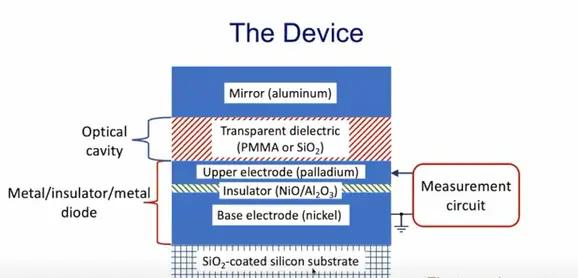
The formation of a submicron optical cavity on one side of a metal–insulator–metal (MIM) tunneling device induces a measurable electrical current between the two metal layers with no applied voltage. Reducing the cavity thickness increases the measured current. Eight types of tests were carried out to determine whether the output could be due to experimental artifacts. All gave negative results, supporting the conclusion that the observed electrical output is genuinely produced by the device. We interpret the results as being due to the suppression of vacuum optical modes by the optical cavity on one side of the MIM device, which upsets a balance in the injection of electrons excited by zero-point fluctuations. This interpretation is in accord with observed changes in the electrical output as other device parameters are varied. A feature of the MIM devices is their femtosecond-fast transport and scattering times for hot charge carriers. The fast capture in these devices is consistent with a model in which an energy ∆E may be accessed from zero-point fluctuations for a time ∆t, following a ∆E∆t uncertainty-principle-like relation governing the process...
https://www.colorado.edu/faculty/moddel/node/229
http://www.youtube.com/watch?v=l7CX89cTvFw&list=PL0F205ADE6845227F
“Something from nothing: An evaluation of vacuum energy extraction methods,”
G. Moddel, Annual Meeting of the Society for Scientific Exploration, May 28-30, Charlottesville, Virginia, 2009.
https://e-catworld.com/2022/02/11/video-extracting-zero-point-energy-does-it-violate-the-second-law-garret-moddel-reports-working-zpe-devices/
“Extracting Zero Point Energy: Does it Violate the Second Law?” (Garret Moddel Reports Working ZPE Devices)
February 11, 2022
Here is a video of a presentation by Garret Moddel of the University of Colorado at Boulder. He was speaking at an online conference hosted by The UnLAB held Jan 18-22, 2022. The full meeting and talks can be accessed here:
https://unlab.us/advanced-propulsion-and-energy-2022/
Some of the key points and quotes from the video:
He asks how much energy is available from the zero point energy field, and based on theoretical calculations based on Planck’s constant he says that the current which is available from the photon flux of the background electromagnetic field is 1.7 GA (giga amps) per square meter.
Two major problems when it comes to extracting this energy:
1. This background energy is the universal ground state: “We can’t induce a flow by having a change in its density because it’s the same everywhere”.
2. The fluctuations in this ZPE are field are very short-lived.
He asks: Can we modify the ground state? And he answers, yes we can – with the Casimir cavity.
He also says that energy may be ‘borrowed’ from the vacuum.
Here’s a slide showing the basic setup of his device:
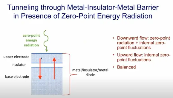
“The basic device consists of a metal insulator, a metal structure . . . The upper insulator is semi-transparent, there is a very thin insulator which allows electrons to tunnel or hop over the barrier, and the base metal is a little thicker.
“So if we imagine this thing just sitting in equilibrium, in steady-state, we’ve got ZPE modes in the base metal, these are dominantly in visible light, and energy, these are dominantly in the form of plasmons, and so these plasmons will have a distribution, there’ll be fluctuations that can create a sufficiently hot electron to go across the barrier to the top metal.
“Similarly, in the top metal there are going to be these plasmons powered by ZPE that will create electrons that can go in the opposite direction, but this top metal is a little bit thinner, so there are fewer of those electrons. On the other hand, there are also the external vacuum enery modes which can energize an electron by the photo-electric effect. That hot electron might be able to traverse this thin metal, go across the insulator and get to the bottom metal. In this way, if we’re sitting in equilibrium, there’s no net flow.
“Now let’s put a Casimir cavity on top, the Casimir cavity blocks the low frequency modes. We’re now going to have fewer electromagnetic modes from the ZP field, so we’ve now broken the balance, we now have net electron flow from the bottom to the top.”
“We are actually producing power in our devices, and the power is substantial. The maximum measured power density is 70 W/m2”
He notes that these are very small devices.
https://www.youtube.com/watch?v=GmLsF5yEd9o&embeds_referring_euri=https%3A%2F%2Fe-catworld.com%2F&source_ve_path=OTY3MTQ
Garret Moddel, SSE Special Session, Jan 22, 2022, Advanced Propulsion & Energy IV
https://www.youtube.com/watch?v=2tGRhTXKh8A
Society for Scientific Exploration
Unlocking Zero-Point Energy
This video describes how the energy is harvested, the practical and scientific implications of this, and what the reaction of the scientific community has been so far.
https://www.mdpi.com/2073-8994/13/3/517/htm
Optical-Cavity-Induced Current
by Garret Moddel, et al.
Abstract
The formation of a submicron optical cavity on one side of a metal–insulator–metal (MIM) tunneling device induces a measurable electrical current between the two metal layers with no applied voltage. Reducing the cavity thickness increases the measured current. Eight types of tests were carried out to determine whether the output could be due to experimental artifacts. All gave negative results, supporting the conclusion that the observed electrical output is genuinely produced by the device. We interpret the results as being due to the suppression of vacuum optical modes by the optical cavity on one side of the MIM device, which upsets a balance in the injection of electrons excited by zero-point fluctuations. This interpretation is in accord with observed changes in the electrical output as other device parameters are varied. A feature of the MIM devices is their femtosecond-fast transport and scattering times for hot charge carriers. The fast capture in these devices is consistent with a model in which an energy ∆E may be accessed from zero-point fluctuations for a time ∆t, following a ∆E∆t uncertainty-principle-like relation governing the process.
Garret Moddel Patents
ENHANCED QUANTUM VACUUM ENERGY DEVICES -- US12166434 [ PDF ]
A device includes a first reflector composed of a first reflector material that is electrically conductive, a second reflector facing the first reflector to form an optical cavity, and an electrode located between the first reflector and the second reflector. The electrode is composed of an electrode material that is both electrically conductive and at least partially transparent. Examples of the electrode material include metal, transparent conductive oxides, semiconductors, and conductive polymers. To harvest energy, a current driven through the device creates a stream of charge carriers that flows between the first reflector and the electrode. The second reflector may also be composed of an electrically conductive material, in which case a second current may be driven through the device to create a second stream of charge carriers that flows between the second reflector and the electrode.
QUANTUM VACUUM FLUCTUATION DEVICES -- US11133758 [ PDF ]
Described herein are devices incorporating Casimir cavities, which modify the quantum vacuum mode distribution within the cavities. The Casimir cavities can drive charge carriers from or to an electronic device disposed adjacent to or contiguous with the Casimir cavity by modifying the quantum vacuum mode distribution incident on one side of the electronic device to be different from the quantum vacuum mode distribution incident on the other side of the electronic device. The electronic device can exhibit a structure that permits transport or capture of hot carriers in very short time intervals, such as in 1 picosecond or less.
SYSTEMS FOR DRIVING THE GENERATION OF PRODUCTS USING QUANTUM VACUUM FLUCTUATIONS -- US11251723 // US11837971 [ PDF ]
escribed herein are systems incorporating a Casimir cavity, such as an optical Casimir cavity or a plasmon Casimir cavity. The Casimir cavity modifies the zero-point energy density therein as compared to outside of the Casimir cavity. The Casimir cavities are paired in the disclosed systems with product generating devices and the difference in zero-point energy densities is used to directly drive the generation of products, such as chemical reaction products or emitted light.
Muscle Optimization Device and Method -- US11793716 [ PDF ]
A device and method are provided for therapy and treatment of biological tissue such as muscle, tendon, and ligament tissue, by use of a device and method in which therapeutic vibrational frequency resonance patterns are transmitted to tissues of a patient. The resonance frequencies originate from many resonance domains, including vitamins, minerals, herbs, amino acids, and fatty acids. Each domain includes therapeutic frequency resonance patterns. These resonance patterns may be passively excited and transmitted to a patient to enhance tissue function, to decrease the normal rehabilitation time of damaged tissue, and provide therapeutic benefits for muscle tissue dysfunction. Therapeutic frequency resonance patterns may also be actively excited by a delivery mechanism that uses electromagnetic or mechanical waves to interact with the device. The actively excited device transmits the therapeutic frequency resonance patterns to the patients for similar enhancements and therapeutic benefits.
QUANTUM NOISE POWER DEVICES -- US11258379 [ PDF ]
Described herein are devices in which quantum noise is reduced, such as by incorporating the devices as part of or adjacent to a Casimir cavity. The devices with reduced quantum noise can be paired with a free-space electric device to allow for a difference in noise power between the two to be captured.
QUANTUM PLASMON FLUCTUATION DEVICES -- US2020357997 [ PDF ]
Described herein are devices incorporating plasmon Casimir cavities, which modify the distribution of allowable plasmon modes within the cavities. The plasmon Casimir cavities can drive charge carriers from or to an electronic device adjoining the plasmon Casimir cavity by modifying the distribution of zero-point energy-driven plasmons on one side of the electronic device to be different from the distribution of zero-point energy-driven plasmons on the other side of the electronic device. The electronic device can exhibit a structure that permits transport or capture of carriers in very short time intervals, such as in 1 picosecond or less.
US11258379 -- QUANTUM NOISE POWER DEVICES [ PDF ]
Described herein are systems incorporating a Casimir cavity, such as an optical Casimir cavity or a plasmon Casimir cavity. The Casimir cavity modifies the zero-point energy density therein as compared to outside of the Casimir cavity. The Casimir cavities are paired in the disclosed systems with product generating devices and the difference in zero-point energy densities is used to directly drive the generation of products, such as chemical reaction products or emitted light.
SYSTEM AND METHOD OF DELIVERING REPLICATED THERAPEUTIC FREQUENCIES BY PULSED ELECTROMAGNETIC FIELD -- WO2018052746 [ PDF ]
A system, device and method are provided for exposing a patient to therapeutic resonant frequency patterns (RFP) for therapy and treatment of a patient, for example, biological tissue such as muscle, tendon, ligament, and nerve tissue. The resonance frequencies originate from many bioactive substances, pharmaceuticals or other compounds, and key frequencies of the RFP of a compound can be replicated and then delivered to a patient using an electromagnetic catalyst to provide therapeutic benefits. RFPs can be imprinted in a separate device using a plasma imprinting device and method. This separate device can be actively excited by a delivery mechanism that uses electromagnetic or mechanical waves to interact with the device. The actively excited device transmits the RFPs or therapeutic resonant frequency patterns to the patient for similar enhancements and therapeutic benefits.
RADIATING POWER CONVERTER AND METHODS -- US9581142 [ PDF ]
An energy conversion device generates electrical power responsive to a flow of thermal power. An energy radiator is in thermal communication with the energy converter and includes an input side for receiving the flow from the energy converter and an output side that is tuned for selectively emitting at least a portion of the thermal flow in a bandwidth at which the atmosphere of Earth is substantially transparent and/or with a sufficiently small radiation angle such that the portion of the thermal flow can be radiated to outer space. In one system, the energy conversion device held at least near an ambient temperature. In another system, the energy conversion device is maintained below an ambient temperature.
SPECTRUM SPLITTING USING OPTICAL RECTENNAS -- US9255840 [ PDF ]
Systems and methods for an improved solar/infrared conversion efficiency using multiple rectennas, one for each band of the spectrum. Each rectenna is optimally efficient for each spectrum band. An antenna receives at least one of a visible or infrared spectrum. Rectifying circuits coupled to the antenna generate a current based on a portion of the spectrum received by the at least one antenna. Each rectenna operates efficiently using a different operating voltage. The operating voltages are based on the selected load resistor and the current-voltage characteristics for the diode of the rectifying circuit at the associated spectrum portion.
Geometric diode, applications and method -- US2011017284 [ PDF ]
A geometric diode, method and device applications are described. The geometric diode is produced including a device body formed from an electrically conductive material having an equilibrium mobile charge density, and having a device surface configuration. The material has a charge carrier mean free path with a mean free path length and the device body size is selected based on said the free pathlength to serve as an electrically conductive path between first and second electrodes delimited by the device surface configuration that is asymmetric with respect to a forward flow of current in a forward direction from the first electrode to the second electrode as compared to a reverse current flow in an reverse direction from the second electrode to the first electrode. A system includes an antenna for receiving electromagnetic radiation coupled with the geometric diode antenna to receive the electromagnetic radiation to produce an electrical response.
Quantum vacuum energy extraction -- WO2008039176 [ PDF ]
A system (fig 2) is disclosed for converting energy from the electromagnetic quantum vacuum available at any point in the universe to usable energy in the form of heat, electricity, mechanical energy or other forms of power. Mode suppression of electromagnetic quantum vacuum radiation, known to result in the emission of energy, takes place in Casimir cavities (10). When atoms enter into suitable micro Casimir cavities a decrease in the orbital energy of electrons in atoms will thus occur. Such energy is captured by the claimed devices (24,26).
High speed electron tunneling devices -- US7595500 [ PDF ]
A detector includes a voltage source for providing a bias voltage and first and second non-insulating layers, which are spaced apart such that the bias voltage can be applied therebetween and form an antenna for receiving electromagnetic radiation and directing it to a specific location within the detector. The detector also includes an arrangement serving as a transport of electrons, including tunneling, between and to the first and second non-insulating layers when electromagnetic radiation is received at the antenna. The arrangement includes a first insulating layer and a second layer configured such that using only the first insulating in the arrangement would result in a given value of nonlinearity in the transport of electrons while the inclusion of the second layer increases the nonlinearity above the given value. A portion of the electromagnetic radiation incident on the antenna is converted to an electrical signal at an output.
Method for fabricating a metal-oxide electron tunneling device for solar energy conversion -- US6762071 [ PDF ]
A method for fabricating an electron tunneling device on a substrate includes forming a first non-insulating layer on the substrate and providing a first amorphous layer. The method further includes the steps of providing a second layer, and forming a second non-insulating layer and providing an antenna structure connected with the first and second non-insulating layers. The second layer of material is configured to cooperate with the first amorphous layer such that the first amorphous layer and the second layer of material together serve as a transport of electrons between and to the first and second non-insulating layers, and the transport of electrons includes, at least in part, transport by means of tunneling.
Electrically isolated semiconductor integrated photodiode circuits and method -- US4612408 [ PDF ]
An interconnected array of solar cell or photodiode devices is formed by a method which includes the steps of forming on one major surface of a semiconductor wafer a plurality of said devices, forming grooves in said one major surface extending partway into said substrate between adjacent said devices, forming an oxide layer on selected portions of said one major surface and on the surfaces of said grooves, filling the grooves with an insulating material, forming metal interconnects between adjacent devices extending over said grooves and insulating material, attaching said one major surface to an insulating support, and severing through the wafer into the grooves from the other major surface to separate adjacent devices while leaving the metal interconnects.
TERAHERTZ DEVICE INTEGRATED ANTENNA FOR USE IN RESONANT AND NON-RESONANT MODES AND METHOD -- US6835949 [ PDF ]
An assembly includes a device for receiving at least one input to produce an output. An antenna supports the device to transfer the input to the device and further to transfer the output from the device such that the antenna supports a selected one of the input and the output as a high frequency current. The antenna includes a peripheral configuration which confines high frequency current to at least one dominant path to oscillate therein. The other one of the input and the output is a lower frequency signal present at least generally throughout the antenna. At least one port is positioned away from the dominant path to isolate the lower frequency signal from high frequency current in the dominant path. The antenna is configured to support the lower frequency signal having a frequency in a low frequency range including zero to several terahertz.
Surface Plasmon Devices -- US7177515 [ PDF ]
An assembly includes a device for receiving at least one input to produce an output. An antenna supports the device to transfer the input to the device and further to transfer the output from the device such that the antenna supports a selected one of the input and the output as a high frequency current. The antenna includes a peripheral configuration which confines high frequency current to at least one dominant path to oscillate therein. The other one of the input and the output is a lower frequency signal present at least generally throughout the antenna. At least one port is positioned away from the dominant path to isolate the lower frequency signal from high frequency current in the dominant path. The antenna is configured to support the lower frequency signal having a frequency in a low frequency range including zero to several terahertz.
Silicon quantum dot laser -- US5703896 [ PDF ]
Dynamic variation in the color produced by a silicon quantum dot laser is achieved by utilizing segmented sections or patches of quantum dots of differing sizes to produce different colors of light. The amount of each color of light produced is controlled by selectively biasing the segments of quantum dots. The light is caused to resonate coherently and is emitted out by a diffraction grating. The dynamic variation in the color of light produced by such a device makes it useful as a multicolor pixel in a color display of images.
Interconnected high speed electron tunneling devices -- US7126151 [ PDF ]
An integrated circuit chip includes a formation of integrated layers configured to define at least one integrated electronic component. The integrated layers further define an integrated electron tunneling device, which includes first and second non-insulating layers spaced apart from one another such that a given voltage can be provided thereacross. The integrated electron tunneling device further includes an arrangement disposed between the first and second non-insulating layers and serving as a transport of electrons between and to the first and second non-insulating layers. The arrangement includes at least a first layer configured such that the transport of electrons includes, at least in part, transport by means of tunneling. The integrated electron tunneling device further includes an antenna structure connected with the first and second non-insulating layers, and the integrated electron tunneling device is electrically connected with the integrated electronic component.
Self-powered optically addressed spatial light modulator -- US5177628 [ PDF ]
A self-powered liquid crystal spatial light modulator is disclosed having a pair of spaced transparent glass plates, on each plate of which a transparent electrically conductive film is coated so as to be in confronting relation. A voltage/current generating, photovoltaic/photodiode, light sensitive layer is coated onto one of the conductive films. A liquid crystal layer is confined between the other conductive film and the light sensitive layer. A shorting circuit element connects the two conductive films. This shorting circuit element may be internal or external to the spatial light modulator. A pixel area of the spatial light modulator is addressed by a beam of light that illuminates the pixel area and operates to activate a corresponding area of the light sensitive layer. The voltage/current that is generated in this area of the light sensitive film causes a current to flow through the shorting circuit element, to thereby activate, switch or charge the corresponding area of the liquid crystal layer. Transmission mode and reflection mode spatial light modulators are described.
Pulse anneal method for solar cell -- US4539431 [ PDF ]
A solar cell including a pulse annealed layer of crystalline, amorphous or polycrystalline semiconductor material of one conductivity type and either a layer of opposite conductivity type or a liquid electrolyte forming a collector junction therewith. A method of improving the characteristics of a solar cell including at least one layer of crystalline, amorphous or polycrystalline semiconductor material which includes the step of pulse annealing said semiconductor material.
Terahertz interconnect system and applications -- US6967347 [ PDF ]
An assembly includes a first electrical circuitry for providing a first electrical signal containing data and a transmitting arrangement, connected with the first electrical circuitry, for receiving the first electrical signal and for converting the first electrical signal into an electromagnetic signal containing at least a portion of the data. The electromagnetic signal has a carrier frequency greater than 300 GHz. The assembly also includes a receiving arrangement for receiving the electromagnetic signal and for converting the electromagnetic signal into a second electrical signal containing at least some of the portion of the data, and a second electrical circuitry connected with the receiving arrangement and configured for receiving the second electrical signal.
Electro-optic wedge structure for beam steering and method of manufacture -- US5615029 [ PDF ]
An apparatus for steering a beam of light. A volume of electro-optic, light transmissive material has a predetermined geometric shape, such as a wedge, and is positioned to intersect the beam of light so that the beam of light is directed into the material. The material has a first surface on which the beam of light is incident and a second surface opposite the first surface, the first and second surfaces defining a portion of the material therebetween having a thickness which varies with the beam of light passing through the portion of the material. A voltage source applies a potential difference across the portion of the material. A control circuit varies the magnitude of the potential difference applied to the portion of the material. As a result, the beam of light is deflected by an angle which is a function of the varying thickness of the portion of the material and the refractive index of the portion of the material as determined by the magnitude of the potential difference.
Light modulating eyewear assembly -- US6760080 [ PDF ]
The present invention, in accordance with one embodiment, provides for a light modulating cell assembly especially suitable as eyewear including a detector and a light blocking arrangement at least partially surrounding a detector for allowing only light from a limited range of ambient directions to directly reaching said detector. In accordance with another embodiment there is a light transmissivity control arrangement including auxiliary means for controlling the state of said light modulating medium.
Quantum vacuum energy extraction -- US7379286 [ PDF ]
A system is disclosed for converting energy from the electromagnetic quantum vacuum available at any point in the universe to usable energy in the form of heat, electricity, mechanical energy or other forms of power. By suppressing electromagnetic quantum vacuum energy at appropriate frequencies a change may be effected in the electron energy levels which will result in the emission or release of energy. Mode suppression of electromagnetic quantum vacuum radiation is known to take place in Casimir cavities. A Casimir cavity refers to any region in which electromagnetic modes are suppressed or restricted. When atoms enter into suitable micro Casimir cavities a decrease in the orbital energies of electrons in atoms will thus occur. Such energy will be captured in the claimed devices. Upon emergence form such micro Casimir cavities the atoms will be re-energized by the ambient electromagnetic quantum vacuum. In this way energy is extracted locally and replenished globally from and by the electromagnetic quantum vacuum. This process may be repeated an unlimited number of times. This process is also consistent with the conservation of energy in that all usable energy does come at the expense of the energy content of the electromagnetic quantum vacuum. Similar effects may be produced by acting upon molecular bonds. Devices are described in which gas is recycled through a multiplicity of Casimir cavities. The disclosed devices are scalable in size and energy output for applications ranging from replacements for small batteries to power plant sized generators of electricity.
Optically addressable spatial light modulator -- US4941735 [ PDF ]
A liquid crystal spatial light modulator is disclosed having a pair of spaced transparent plates on which two electrically conductive films are coated in confronting relation. A continuous or discontinuous photosensitive film is coated on one of the conductive films. A bistable ferroelectric liquid crystal is confined between the other conductive film and the photosensitive film. An activating voltage source is applied to the conductive films. Modulator pixels are defined by a plurality of small electrically conductive elements that are carried by the photosensitive film. These conductive elements may be either transparent to a reading wavefront, or they may be reflective to a reading wavefront. An apertured film is also mounted on the photosensitive film substantially coplanar with the conductive elements. The apertures in this film coincide with the positions of the conductive elements and are spaced therefrom, to thereby leave a ring-shaped area of exposed photosensitive film surrounding each reflector element. A plurality of opaque rings are carried by said other conductive film, so as to overlie the ring-shaped area of exposed photosensitive film that surrounds each conductive element. Individual pixels of the modulator are addressed by light activating the portion of the photosensitive film that is associated with the addressed pixel's individual conductive element. Photodiode and photoconductive pixel cells are disclosed.